How Do Flex PCBs Handle Exposure to UV Radiation?
Flex PCBs Handle Exposure to UV Radiation
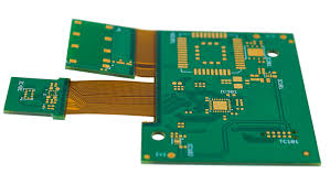
Designed to be flexible and durable, flex PCBs feature a base material that can bend and fold. They are used in a wide range of applications, from heads-up displays for aviation piloting and wearable technology to minuscule devices like medical scanners and pacemakers. In addition, flex circuits can also absorb vibrations and other external forces better than traditional rigid PCBs. They can also be made more compact to fit into the final device, reducing overall size and weight.
Unlike their rigid counterparts, flex PCBs are manufactured on thin substrates of polyester or polyimide. Conductive material traces are etched on the substrate in as many layers as the PCB design calls for. The layers are then coated with a protective coverlay that protects the exposed copper and reduces electrical interference from dirt, moisture, and other potential damage.
The thickness of the substrate varies depending on the flex circuit’s intended flexibility. Thicker materials are more durable, but they also cost more to manufacture. Consequently, thinner flex pcbs are often found in smaller, less expensive electronic devices.
How Do Flex PCBs Handle Exposure to UV Radiation?
To ensure that a flex PCB can handle the stresses of its environment, the designers must carefully select appropriate materials and layouts for the circuit. For example, it is important to keep the number of conductors on a flex PCB to a minimum, and to avoid routing them across areas where stress is expected. Also, the traces should be routed in such a way that they are not subjected to excessive bending or twisting. This means that the designer must select curve traces instead of straight ones, and avoid changing the width or direction of the conductors when they are bent.
Another consideration is that flex PCBs must be made from high-grade materials with low dimensional stability. They must also be protected from chemicals, oils, and ultraviolet radiation, which can all degrade the materials. A stiffener, which is a small strip of rigid material, can be added to selected regions of the flex PCB to give it additional mechanical strength.
Flex PCBs are particularly well suited to use in the medical industry. They are used in diagnostic monitors to check blood pressure, glucose, and heart rate. They are also used in medical imaging devices to capture and analyze images for diagnostic purposes. Moreover, flex PCBs are used in LED lighting to divert heat away from bulbs, enabling light fixtures to be more compact.
The fabrication process begins with stacking various layers of the flex circuit board, which is known as the “stack-up”. Each layer is then deposited with copper using a chemical treatment. Then, the conductive material is etched on each layer using the desired pattern. The etching process can be assisted with the use of masks and stencils to accurately deposit the desired pattern. Once the etching is complete, it’s time to solder the components. The finished flex PCBs are then tested for connectivity and other parameters. The PCBs are then cleaned and inspected before being shipped to their intended customers.