The 3 Steps in the Circuit Board Assembly Process
Circuit Board Assembly Process
Printed circuit board (PCB) assembly is an important step in making electronic devices that consumers can use. It requires rigorous testing and inspection, which can be costly for businesses that depend on high-quality products for their livelihood. PCB assembly is also an important component in preserving the integrity of a device and ensuring its long-term reliability. Advanced assembly techniques, effective PCB protective coatings and stringent quality control all contribute to this goal.
Before manufacturing begins, a company that specializes in PCB assembly will run a Design for Manufacture (DFM) check to ensure that the design meets all necessary requirements. This helps prevent unforeseen issues that could negatively impact the functionality of the final product.
Once the DFM check is complete, the circuit board assembly process starts with the creation of a photo film. A special kind of printer known as a plotter uses the photo film to create a plan for the copper paths on the board. Each layer of the PCB gets its own separate sheet, and the layers are aligned by punching precise registration holes in each film. This makes it easy for assemblers to know which sections of the board will require solder paste.
The 3 Steps in the Circuit Board Assembly Process
Next, a machine drills holes into the bare board where components will go. Then the panel is bathed in a series of chemicals that fuse all the different layers together and make it ready to be assembled. This is followed by a process called electroplating, in which the copper is deposited onto the panels and into all the holes that were drilled.
After the copper is plated, it’s cleaned again and inspected for defects using a technique known as Automated Optical Inspection (AOI). A special camera examines each panel for flaws such as missing or extra connections, which can be corrected during the assembly process.
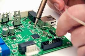
The last step in the circuit board assembly process is component placement. Traditionally, this was done manually by professional engineering staff, who used a pair of tweezers to pick and place small components on the PCB. However, this process has been automated for higher volume production. This has lowered costs while maintaining accuracy and consistency. It also reduces the risk of error caused by fatigue and eyestrain, which is a common problem among humans working with such tiny components.
Once the component placement is complete, the assemblers begin to solder them into place. Depending on the size of the circuit boards, this may involve wave or reflow soldering. The assemblers are careful to match the polarity of each component as well as its orientation to ensure proper functioning once the circuit is completed. In addition, they must adhere to all relevant regulations and operation standards for the device. Finally, the finished circuit boards are tested for quality and functionality. This includes a variety of tests such as vibration, shock and thermal stresses, which can be quite severe for electronics like tablets, smartphones and digital cameras. These tests ensure that the circuit board will be able to withstand the stress of everyday use.